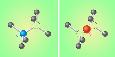
In recent years, diamond has emerged as a promising material for solid state quantum optics due to the presence of optically active point defects or so-called color centers. In particular, the negatively charged nitrogen vacancy (NV), and silicon vacancy (SiV) centers provide electronic and nuclear spins, which can be initialized, manipulated and read out via optical and microwave fields.
| Molecular structure of NV and SiV centers |
 |
These optically accessible spin qubits can function as a spin-photon quantum interface, and can be used to realize entanglement of spins located kilometers apart, which is a key resource for quantum networks. However, building efficient interfaces between light and matter qubits requires strong light-matter interactions. The key approach towards this goal is cavity quantum electrodynamics (cQED), in which these atom-like systems are made to interact strongly with photons in optical cavities.
To this end, our lab has pioneered the development of diamond nanophotonics. Via our diamond angled etching and thin film nanofabrication techniques, developed over the years (see section on Diamond Nanofabrication), we can fabricate a variety of nanoscale optical devices in single crystal diamond. In particular, our photonic crystal nanobeam cavities provide high quality factors, and wavelength scale optical mode volumes for enhanced interaction strength between photons and diamond color centers [Nature Commun. 5, 5718 (2014)].
| Angle etched photonic crystal nanobeam cavities in diamond |
 |
| Diamond nanowire array, and corresponding confocal microscope image showing fluorescence from single NVs in the wires |
 |
Our initial efforts on diamond quantum photonics with NV centers focused on improving photon collection efficiency [Nature Nanotech. 5, 195 (2010)], and enhancing emission of coherent optical photons in the zero phonon line by coupling them to nano-cavities [Nano Lett., 12 (3), 2012]. Our NV-diamond nanowire devices with NV centers have found application in sensing as high spatial resolution scanning probe magnetometers [Nature Nanotech. 7, 320 (2012)].
| Targeted implantation of SiV centers in diamond nanobeams |
 |
More recently, we have exploited the favorable optical properties of SiV centers, and the capability to deterministically position them in nano-cavities to realize a cQED based single photon switch [manuscript in preparation]. Our ongoing efforts towards next-generation devices include fiber-integration to develop an on-demand high bandwidth single photon source, which can have far-reaching applications in linear and nonlinear quantum optical computing. In particular, this will enable high bandwidth spin-photon entanglement generation, which is essential to realize multi-node quantum networks.